On one of the usual sources of weird electronics I came across quiet unusual SFP+ module and could not resist buying it to see how it works. For now I was unable to make it work, but at least I made few photos of its internals. It turned out its main part is obscure chip made by Semtech and described as GN1157, which serves as laser diode driver. Obviously obtaining datasheet is impossible even in China. However, thanks to being able to see the board, I was able to reverse engineer some part of its pinout. Continue reading “Pinout of laser driver for CPRI SFP+ module – GN1157”
Tag: electronics
My small library of KiCAD footprints
This time just a quick info. I just published library of KiCAD footprints that I made recently for my new project. The project itself has not been published yet and I want to keep it that way until I get first working prototype (what I hope will happen really soon). Meanwhile I am publishing this small library of footprints that I made for it with perspective of extending it in future with other hardware projects.
Still this is quite new topic for me as I have no electronics education, nor professional experience, so there is still a risk that I may fail at what I do and abandon such kind of projects. But for now, I just finished validation of footprints published here with a board that I ordered from JLCPCB, so you are guaranteed that they are fine (except one marked explicitly as such). Continue reading “My small library of KiCAD footprints”
New VCI+A-BT (DS150E) ST-Link pinout
This device could easily be found at the Chinese sellers. They advertise them as DS150E. Under the hood there is nice STM32 and STM8 pair. One is present on main PCB (in my case TCS MAIN V6.0), the other on relay board (TCS+RELAY V3.0). Both chips have their ST-Link headers broken out. If one want to read/write the firmware installed in internal flash, it should be as easy as connecting few of these pins. Continue reading “New VCI+A-BT (DS150E) ST-Link pinout”
mhz14a – program for managing MH-Z14/MH-Z14A CO2 sensors via UART
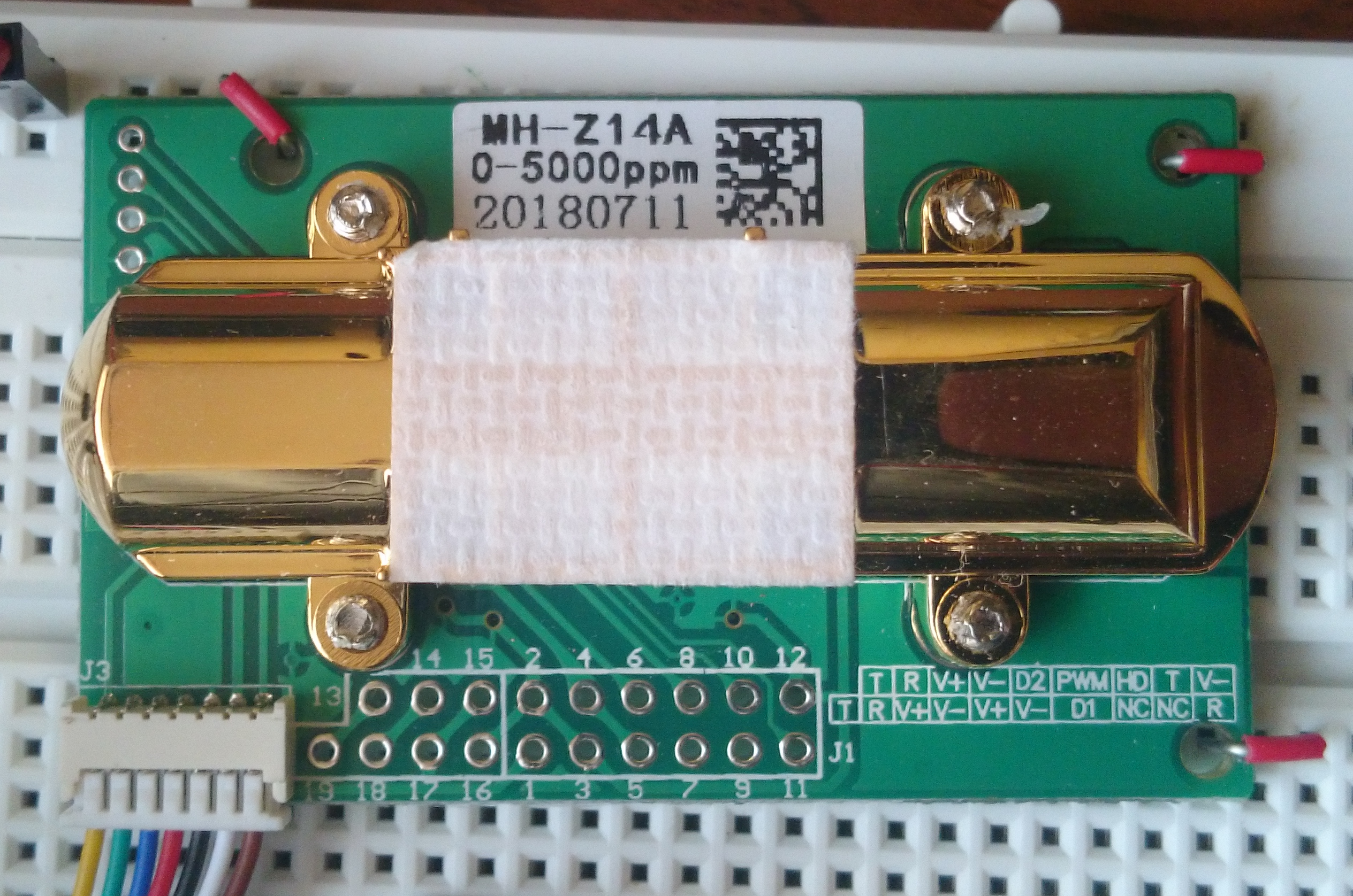
When I have seen CO2 sensor for the first time, it was quite expensive device. Well, if one want to buy consumer device these days, it still could cost a lot. However in the days of cheap Chinese electronics sellers on biggest auction platforms, for makers, situation is quite different now. MH-Z14 is the cheapest CO2 sensor I was able to find. I costs about $19 and comes in few variants: MH-Z14 and MH-Z14A. Also it can measure up to 1000 ppm, up to 2000 ppm or up to 5000 ppm. However the range does not matter in practice, as it is possible to switch between them using UART.
The device interfaces are quite flexible for such a cheap device, as beside mentioned UART port it provides PWM and analog output. However, I was not able to measure valid value using analog and my cheap multimeter. Maybe some more sophisticated equipment is required for that.
I have to make one note here: device I bought is labeled as MH-Z14A and its range is 0-5000 ppm. Other variants might have different features. For mine, there is no UART protocol documentation. Yet, protocol documented under name MH-Z14 works, so be careful. Continue reading “mhz14a – program for managing MH-Z14/MH-Z14A CO2 sensors via UART”
[Import]Understanding JCOP: pre-personalization
NOTE: This post was imported from my previous blog – v3l0c1r4pt0r.tk. It was originally published on 25th July 2017.
As I promised some time ago, now I am going to describe process of pre-personalization of a JCOP card. JCOP is one of the easier to get JavaCard-compatible cards. However they cost a bit. The problem with the ones available from eBay sellers is lack of pre-personalization. Ok, there are some advantages of buying not pre-personalizaed card, like ability to set most of its parameters, but by the way it is quite easy to make such card unusable.
Online resources, as I mentioned in the first part of the tutorial, are not very descriptive. They say that there is such thing like pre-personalization and it has to be done before using the card, flashing applets, using them and so on. There is only one source that helps a little bit. Someone has written script for the process. However there are two problem with the script. The first one is that it is written in some custom language and internet does not know about the interpreter, it is probably something provided by NXP – manufacturer of JCOP for its customers and neither me nor (probably) you, reader, are their customers. The consequence is that we can have script in custom language, with commands like ‘/select’ or ‘/send’. Fortunately, documentation of ISO 7816 (smart card connection), allows to decipher this. So this problem could be finally solved. Another problem is lack of command values and addresses in memory, so we do not know where and how to read/write/execute anything. After really deep search in Google, finally, I was able to find out all the missing values, so this tutorial could be written.
Process overview
Ok, after this way too long historical introduction, let’s see what will be needed. I assume, you are already able to communicate with your card using raw PDUs. If you don’t, up to this point there are quite a few resources to learn from, so I will not describe this. The most important thing here is to have so called transport key (KT). If you do not have it, go get it now. Seller should provide it to you, and if he did not, you are stuck, since the first step requires this key.
So, basically steps will be as follows:
- Select root applet with Transport Key
- Boot the card
- Read/write some data
- Protect the card
- Fuse it
Easy? Easy. But only if you know some hex numbers. Ok, here, one big WARNING: the last step is irreversible and can be done by mistake quite easily, so think twice before sending anything, and if you are sure, that you are done, think twice again, before issuing it.
Pre-personalization, step by step
At first, we use Transport Key to select proper applet. Format of SELECT command is as below:
CLA=00 INS=A4 P1=04 P2=00 Lc=10 (...)
Where CLA is always zero, INS means SELECT, P1, according to ISO7816 means selection by DF name and Lc is length of KT. After that, key have to be appended. Of course, whole APDU is to be given to communications program as binary values or hex values only.
What now follows is specific to NXP cards only and is mostly undocumented publicly. First of such commands is BOOT command. Its format is as follows:
CLA=00 INS=F0 P1=00 P2=00
Now double care have to taken, because FUSE command should be available after this point and its APDU consists only of zeros, so every mistake might make the card unusable, since security keys are generated randomly for each card.
Reading memory
Now the most important values to read are called CM_KEY and GPIN in memory dump, I shared in the previous post on the topic. First one starts at offsets: 0xc00305, 0xc00321 and 0xc0033d and are 0x10 bytes long. The other one can be found at offset 0xc00412 and by default should be 5 bytes long. However maximum length is also 0x10, so it is better to make sure the length is really 5 by reading byte at offset 0xc00407. To sum up following commands need to be issued and results be saved for future use:
CLA=C0 INS=B0 P1=03 P2=05 Lc=10 C0 B0 03 21 10 C0 B0 03 3D 10 C0 B0 04 07 01 C0 B0 04 12 xx
Where CLA + P1 + P2 is concatenated address of memory area to read, INS=B0 is read command and Lc contains length of data to read.
Writing data
Alternatively, it is possible to write custom values to these buffers. This is especially encouraged for users who want to use the card not only for testing. Overwriting the values could be done with following:
CLA=C0 INS=D6 P1=03 P2=05 Lc=10 (...) C0 D6 03 21 10 (...) C0 D6 03 3D 10 (...) C0 D6 04 12 05 (...)
Where user data is filled with some random data of length in Lc field.
Required values
Beside securing keys, it is required to set CM_LIFECYCLE value to 0x01 and make sure all fields related to keys and PIN have proper values. Here, my memory dump can be used as reference, since I initialized the card before dumping the memory.
Finishing
After setting all the fields to desired values, there are two more steps to do. First one is issuing PROTECT command. It looks as below:
CLA=00 INS=10 P1=00 P2=00
And finally, sending FUSE command with:
CLA=00 INS=00 P1=00 P2=00
Here again, remember, that this command cannot be undone!
Well done! Your card should now be pre-personalized and ready to use, even in production environment. At the end, one remark: probably FUSE command does not need to be issued at all. However, if it is not issued, the card is completely insecure and should not be used in production.
Previous part of this tutorial can found under this link.
[Import]Understanding JCOP: memory dump
NOTE: This post was imported from my previous blog – v3l0c1r4pt0r.tk. It was originally published on 8th February 2017.
Some time ago I was struggling with JCOP smart card. The one I received as it turned out was not pre-personalized, which means some interesting features (like setting encryption keys and PIN) was still unlocked. Because documentation and all the usual helpers (StackOverflow) were not very useful (well, ok, there was no publicly available documentation at all), I started very deep search on Google, which finished with full success. I was able to make dump of whole memory available during pre-personalization.
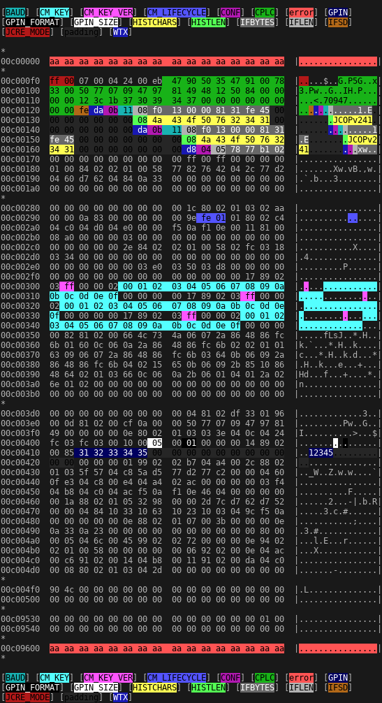
Since it is not something that could be found online, here you have screenshot of it, colored a bit with help of my hdcb program. Without documentation it might not be very useful, but in some emergency situation, maybe somebody will need it.
Small explanation: first address, I was able to read was 0xC000F0, first address with read error after configuration area was 0xC09600. I know that, despite of lack of privileges some data is placed there.
There are three configurations: cold start (0xc00123-0xc00145), warm start (0xc00146-0xc00168) and contactless (0xc00169-at least 0xc0016f). Description of coding of the individual fields is outside of the scope of this article. I hope, I will describe them in future.
Next time, I will try to describe the process of pre-personalization, that is making not pre-personalized card, easy to get from usual sources of cheap electronics, able to receive and run applets.
Update: Next part of this tutorial can be found under this link.
[Import]Airlive WN-151ARM UART pinout & root access
NOTE: This post was imported from my previous blog – v3l0c1r4pt0r.tk. It was originally published on 24th November 2015.
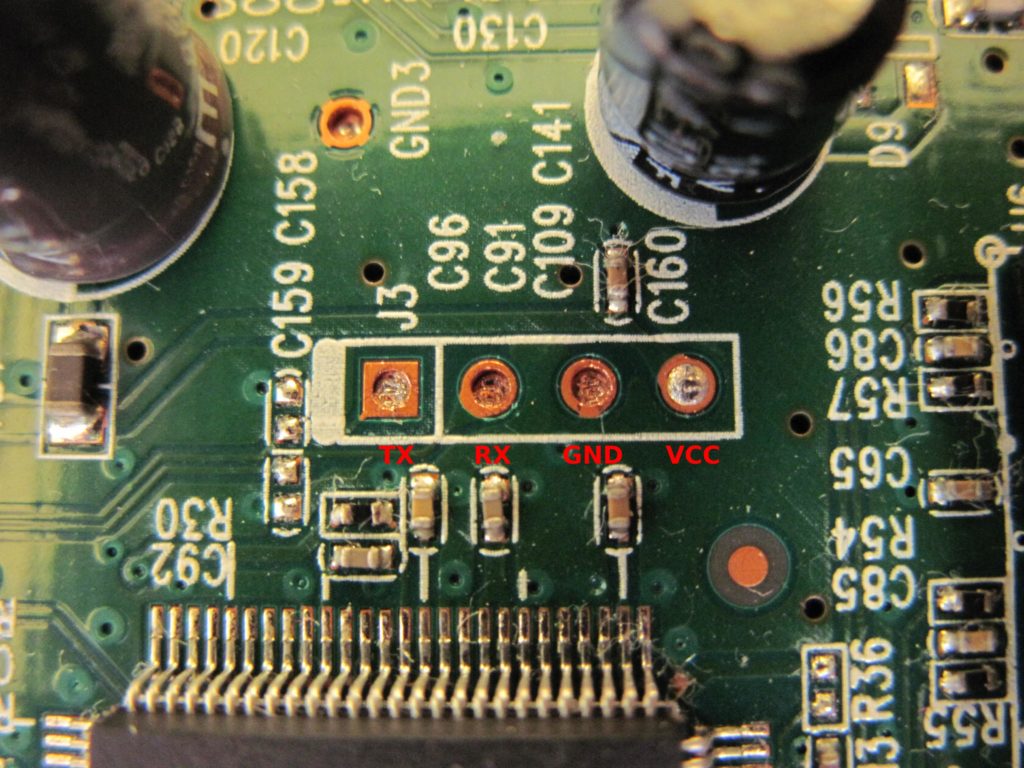
For curious ones. Here is pinout of serial connection. As you can see UART pins are at J4 header (should have pin 4 labeled and 1 be square).
Num. | Function |
---|---|
1 | VCC |
2 | RX |
3 | TX |
4 | GND |
Edit: Oh, and one more thing: goldpin header, you see in the picture is soldered by me, so do not be surprised if you have to hold wires all the time during the transmission.
Root access
There is also possibility to gain root access without removing the cover and possibly voiding the warranty. You have to connect to router’s AP and enter
http://192.168.1.254/system_command.htm
into your browser (panel authentication required). Now you can execute any command you want with root privileges! So let’s type
/usr/sbin/utelnetd -d &
into Console command field and press Execute button. If everything went well, you should now be able to connect to your router using telnet at its default TCP port 23. After that you should see BusyBox banner and command prompt.
It is worth noting that this hidden console cannot be accessed by unauthorized person, so only router administrator can use this (in theory, in practice there are surely a lot of routers using default credentials and security of httpd binary is unknown).
[Import]TP-Link TD-W8901G UART pinout
NOTE: This post was imported from my previous blog – v3l0c1r4pt0r.tk. It was originally published on 31st May 2014.
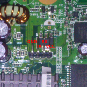
Some people might wonder: what is the pinout of my router’s serial connection. If you’re a happy owner of TP-Link TD-W8901G and asking that yourself, here is the answer:
In the link below there is also this router’s pinout and moreover author states that to make that port working there is a need to modify some resistors. I have V3.5 of that router and didn’t notice any mod to be necessary.
It is possible to solder goldpins in here and router so far haven’t fried. Of course you can try communicating without stable connection and it even works but after training your fingers while waiting for the firmware download/upload to complete you’ll change your mind, I guarantee:).
PS: that model is the one that was one of the victims of massive DNS changing some time ago so if this is the one you’re using as your bridge to the Internet you may be also interested in this.
PS2: if you have another router and want to find out what is the serial port pinout I recommend going here.
[Import]Graphic LCD based on ST7565 chip under Raspberry Pi
NOTE: This post was imported from my previous blog – v3l0c1r4pt0r.tk. It was originally published on 25th December 2013.
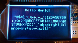
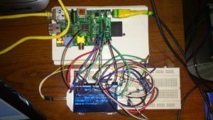
Hi, today I’d like to show you how to connect and use gLCD module with Raspberry Pi as host. The display I have is only bare display without any board not like the one in Adafruit’s offer. It can be powered by 3V3 Raspberry but the display itself needs a bit more power so we will need a few capacitors to build a circuit for that purpose. It will also make the connection a bit complicated (can be seen in the photo on the right). Nevertheless I think that the process is still rather easy.
Overview
As far as I know ST7565 based displays can be connected on two ways: parallel and serial. In case of serial connection, which I used to save few GPIO’s, it is possible to program it using SPI or just only GPIO’s. The display that I have is a bit different than most of the others because it has external backlight, which is additionally single LED so it is very power-saving (15mA). The only problem with that backlight was that the vendor didn’t told anything about parameters of that diode so I needed to figure it out myself.. The second problem while connecting the display itself might be amount of cables that need to be connected when using breadboard. Despite these two facts the whole process should be easy.
Physical connections
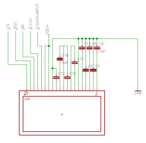
As said before the only step that may be a bit complicated is connecting so called step-up voltage circuit, made of 4 capacitors. The capacitors that we will use are 1uF electrolytic caps. Beside that we need to use another 5 caps (same as before) to connect parallel inputs to ground. So in sum we need 9 of them. Now we only need to connect VDD to 3V3 pin on Raspberry, ground from the schematic on the right with GND pin, SDATA to SMOSI on Pi, SCLK to SCLK and A0, RST and CS to any free GPIO. It is good to remember their numbers cause we will need it in a moment 🙂 It is important to use numbers used by Linux kernel, not wiringPi which has its own names. At last we need to connect the backlight. As said I have ECO backlight so I had to connect mine using 10 Ohm resistor. You can connect it to 3V3 or if you like to have control during runtime use GPIO, just like any other LED.
Configuring the program
Now I have to mention something about a program itself, because depending on how your vendor implemented the things your display will almost surely need a bit different settings. General procedure will look the same on every ST7565-based display. Main differences will be on particular commands during setup procedure.
uint8_t init() { if (!bcm2835_init()) { return 0; } bcm2835_gpio_fsel(LCD_BACK,BCM2835_GPIO_FSEL_OUTP); //backlight bcm2835_gpio_fsel(LCD_A0,BCM2835_GPIO_FSEL_OUTP); //A0 bcm2835_gpio_fsel(LCD_RST,BCM2835_GPIO_FSEL_OUTP); //RST bcm2835_gpio_fsel(LCD_CS,BCM2835_GPIO_FSEL_OUTP); //CS bcm2835_gpio_write(LCD_CS,HIGH); //set CS to high to indicate the bus as free bcm2835_gpio_write(LCD_RST,LOW); bcm2835_delayMicroseconds(1); bcm2835_gpio_write(LCD_RST,HIGH); //hardware reset //setup SPI bcm2835_spi_begin(); bcm2835_spi_chipSelect(BCM2835_SPI_CS_NONE); //manual CS control bcm2835_spi_setClockDivider(BCM2835_SPI_CLOCK_DIVIDER_4); //set speed to 62.5MHz (fastest supported) int i; bcm2835_gpio_write(LCD_CS,LOW); for(i = 0; i < sizeof(initcmd)/sizeof(uint8_t); i++) transfer(initcmd[i],0); bcm2835_gpio_write(LCD_CS,HIGH); bcm2835_gpio_write(LCD_BACK,HIGH); //turn backlight on return 1; }
I think that the code above should be generally clear. The most important for us is for loop that is executing every byte from initcmd array. Its content will look like that:
const uint8_t initcmd[] = { 0xa1, //screen orientation 0x41, //set starting line 0xc0, //page count direction 0xa3, //1/7 bias 0x2c, //vc 0x2e, //vc+vr 0x2f, //vc+vr+vf 0x24, //voltage regulator (0x20-0x27) 0xa6, //do not reverse the display 0xaf, //display on 0xa4, //display from ram 0x81, //turn on brightness regulation 0x18 //set brightness (0x0-0x40) };
The most important values here are:
- voltage regulator – 0x20 means the darkest, as seen above in my case 0x24 worked
- bias – I saw displays that had 1/9 so you need to make sure how is in yours and set it according to chips documentation linked at the end
You may also want to play with commands like screen orientation, page direction, display reverse or brightness to fit them to your needs. Now you have tell the program which GPIO you used as backlight (if you weren’t using GPIO you will now need to comment out few lines that sets backlight up), CS, RST and A0.
The program itself
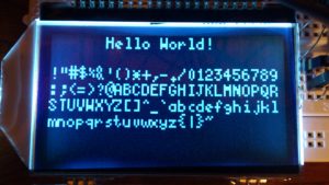
To compile the program you will need to use external library named libbcm2835. It can be installed on ArchLinux ARM by issuing pacman -S libbcm2835 as root. If you are ready you can compile the program by typing: gcc -o lcd lcd.c -lbcm2835 assuming you didn’t change the filename. The simple program I’ve written, basing on the one posted on Gist by tmeissner here and ST7565’s documentation supports transferring single byte (commands too), whole framebuffer, or writing 5×8 single ASCII character or character string. Basing on both codes: mine and Meissner’s I think it is possible to do anything you could think about with that display.
Font creation
Ending slowly it’s time to tell something about fonts. As I said it is possible to simply write characters on the screen. To understand how all that thing works you need to know how the pixels are transfered to the display. The best explanation of the ST7565 display’s work can be in my opinion found here. TL;DR: the whole pixel space is divided into eight, 8-pixel high, horizontal pages divided into 128 columns that are 8 pixels high. If you didn’t understand, try link above. Nevertheless single letter is 8-pixel high and 5-pixel long so we need 5 bytes to store one letter. Its pixel map starts at left, top corner so it’s our (0,0) point and setting LSBof the first byte lights highest pixel. The font that is available in the code is Fixed 5×8 if someone is curious, it’s one of the default fonts in Xorg. To speed up conversion of the font to the display’s format I made simple OpenGL program to do the job for me. The code is of course available to download (check out my github).
DLs
Traditionally, at last some downloads:
- First, and most important: C code of my program
- ST7565 documentation can be found here