This article is part of series about reverse-engineering LKV373A HDMI extender. Other parts are available at:
- Part 1: Firmware image format
- Part 2: Identifying processor architecture
- Part 3: Reverse engineering instruction set architecture
- Part 4: Crafting ELF
- Part 5: Porting objdump
- Part 6: State of the reverse engineering
- Part 7: radare2 plugin for easier reverse engineering of OpenRISC 1000 (or1k)
In the first part, I identified two main problems for further development. First one is unidentified checksum, appended to the end of firmware image. Second one is unknown LZSS-like compression algorithm, used to compress machine code of application processor’s firmware.
Encoder firmware
The thing that till now was more or less unexplored is encoder firmware. LKV373A consists of two processors – application processor using the firmware analyzed in first part and encoder, which reversing I am going to push forward with this article.
Target frmware that I am working on is called LKV373A_TX_V3.0c_d_20161116_bin.bin and is obtainable from danman’s firmware collection.
At first, encoder firmware looks completely different than ITEPKG. The latter was completely structured. This one starts with some data fields, then there is big block of randomly looking data, interlaced with some strings. At the end is familiar SMEDIA02 structure. And this block of “random” data is our target.
First idea I had was running binwalk with -A switch to look for some known opcodes. With no luck. But if we look closer, it seems that this in fact is some kind of machine code.
Finding target

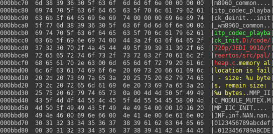
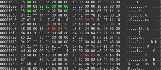
Ok, what we know now is that in firmware image there is a region with many strings written one after another, like on the first hexdump. In another place there is quite a lot data where some of the words are similar to the other. One such fragment can be seen on another hexdump.

So, we can guess, there is code region around 0x81680 and code region near 0xbbc70. Now the question is: how to prove it.
Before proving our hypothesis, one thing is worth noting. If we are right and bytes here are really machine code, then we can be almost sure that instructions are always (or almost always) encoded into 32-bit numbers. That fact is very useful, when we will try to find candidate architectures to test against our characteristics.
How to prove it?
Fortunately, we can see one interesting candidate string. There is some debug message marked in red on data region. If our guess is valid, we should find some reference to it and moreover we can expect there would be only one reference to that particular string.
But now, there is another problem. How to find reference to string, saved somewhere in memory, at offset we have no chance to guess? Now the experience with any machine code might be useful. Usually assembly mnemonics are translated more or less in a form they are written by programmer. So, if we have hypothetical instruction:
add $1,$2+0x1234
Chances are it will be translated to something like:
0x21 0x01 0x02 0x12 0x34
Where lengths of any of these fields and maximum offset possible to write depends on particular architecture.
We can make another assumption. Usually if persistent memory (like EPROM) finally is mapped to operational memory, usually nobody designs device the way, where start of some section is not at address, padded to i.e. page size. So, if we are lucky final address of string in memory should have same least significant bits as our firmware image.
Then, connecting the dots, we can try searching firmware for let’s say two least significant bytes of string offset (0xbcc8). One more remark here: we still don’t know endianness of the processor. And what is worse, after reading firmware format description we don’t know it even more. So we have to check both variants.
Of course, it might happen that in case of different firmware for completely different architecture, all that might fail. There is only one advice to succeed with such analysis: be creative!

The first impression is that I was wrong. There are in fact 5 hits. But… If we look at general firmware structure, we can see that most of the hits are inside SMEDIA container, which as I described in previous post about reverse engineering LKV373A consists of mostly compressed data, and unlikely has any uncompressed code. So, success! We have only one hit inside area we suspected to be code.
By the way we know more than the area is in fact code section. We see that numbers in machine code are stored as big endian. And as we can, we can use 16 bits as offset here. That further narrows number of possible architectures. For instance, popular ARM architecture is little endian, so it is not likely to be used in this case.
I’ll leave as an exercise verification that we are right on another strings present in this firmware.
Further guesswork
Next thing that might ease things a bit is finding out what is a whole format of instruction, that is:
- how many bits are used for opcode?
- how many operands we can use?
- how many bits encode an operand?
When I was doing the work I was not experienced enough to see it from plain word we already have. Then my approach was to guess meaning of 0xA8 opcode we see. As we know that it points to string in possibly write-protected memory, we should not expect it to perform any arithmetic or logic operations. It is rather likely to get pointer of string and store somewhere. Since architecture gives us only 32 bits to use per instruction it is not likely to copy memory somewhere. For me most probable operation is computation of string address, based on some base register and storage in another register. Therefore, I will call the operation: “Load Address” (abbreviated “la“).
Because that information alone does not give us any more hints, but can be used to match our mysterious architecture to one of the known ones, it is high time to do even more guesswork.
Specification matching
Wikipedia has quite useful page, that might help us. But, at first it is good to check some popular ones to see if they match.
As an example, I will use MIPS architecture. It is often used in embedded systems and was quite popular in routers, especially in past, when they were not running Linux. Furthermore it is the most popular architecture that might be big endian, so seems like perfect first check.
Now, we can find some hints on Wikibooks. On MIPS there is instruction format that might match our characteristics.
| opcode | rs | rt | imm |
|---|---|---|---|
| 6 bits | 5 bits | 5 bits | 16 bits |
After search in MIPS manual (its name is “MIPS32™ Architecture For Programmers Volume II: The MIPS32™ Instruction Set” and is probably no more available on original source, but rather some random sites, so no link here), we can see that instruction that has first 6 bits of a word matching our target (0b101010) is “Store Word Left” (swl), so it is not really what we expected.
Now, we have to move on and check another architecture, and another, and another, until we decide we can’t find anything matching. Or finally we will find something. In my case the result is fail. I checked:
- MIPS
- ARM
- ARC
- RISC-V
- PowerPC
- SPARC
- MicroBlaze
- Xtensa
- IBM S/390
- Motorola 68k
- DLX
- Mico32
- LEON
- OpenRISC
- NIOS II
- m32r
And nothing matched. So architecture here is something really uncommon. Because the device is probably performing HDMI signal processing beside being normal processor, it is likely it is in fact soft processor, programmed into some FPGA. Therefore it is likely, finding the architecture documentation will be impossible.
Decoding instruction format
Then we can try another approach. Let’s play a little bit and try to decode rest of instruction using above MIPS I format. First 6 bits means instruction opcode (0x2A or 0b101010), next are two 5-bit fields meaning destination and source register, so we have register 3 for destination and register 3 for source. That definitely makes sense!
So, our hypothesis is that we have 6-bit opcode, 5-bit operands and 16-bit offset encoding. Here, again proving that fact is left as an exercise for the reader.
Going back to our target instruction, we now know that it is executing code like that:
$3 = $3 + 0xbcc8
We will denote this instruction as:
la $3,$3+0xbcc8
What we know?
Now, to sum things up, we learned following things about device’s architecture:
- 32-bit (4-byte) static instruction length
- big endian
- 6-bit opcodes (maximum number of opcodes is 0x40)
- 5-bit operands (32 general purpose registers available)
- indirect addressing of up to 65535 bytes (0xffff)
What next?
As we know quite a lot information about the architecture, we can choose one of the two ways: try to find out what is the name of the architecture and find its documentation (not likely to succeed) or reverse engineer as much instruction as we can. My choice probably will be the latter and if I will succeed in pushing knowledge forward, I will try to describe the process in next article in series.
